Advanced VLSI Design

Instructor
Sujata Dawn
- Description
- Curriculum
- Reviews
This 40+ hour interactive online course provides in-depth knowledge of Advanced VLSI Design, covering ASIC and FPGA architectures, RTL design, CMOS circuits, Physical Design, Static Timing Analysis (STA), Clock Tree Synthesis (CTS), Design for Testability (DFT), low-power design, and emerging semiconductor technologies. Gain hands-on experience with leading EDA tools including Cadence, Synopsys, Xilinx Vivado, and Mentor Tessent while working on real-world RTL-to-GDSII design flow projects. Ideal for students and professionals pursuing careers in ASIC design, FPGA development, Physical Design, Verification, and next-generation semiconductor engineering.
Course Objectives
✓
Master Advanced VLSI Design: Learn CMOS design, ASIC development, FPGA implementation, and modern semiconductor architectures.
✓
RTL-to-GDSII Design Flow: Understand the complete VLSI design process from RTL coding to physical implementation and tape-out.
✓
Physical Design & Timing Analysis: Perform floorplanning, placement, routing, CTS, STA, and power optimization for high-performance chips.
✓
FPGA & Hardware Design: Develop digital systems using Verilog, VHDL, FPGA implementation, and hardware verification techniques.
✓
Design for Testability: Learn DFT methodologies, Built-In Self-Test (BIST), scan insertion, and advanced VLSI testing concepts.
✓
Industry Projects: Gain practical experience using industry-standard EDA tools through real-world semiconductor design projects.
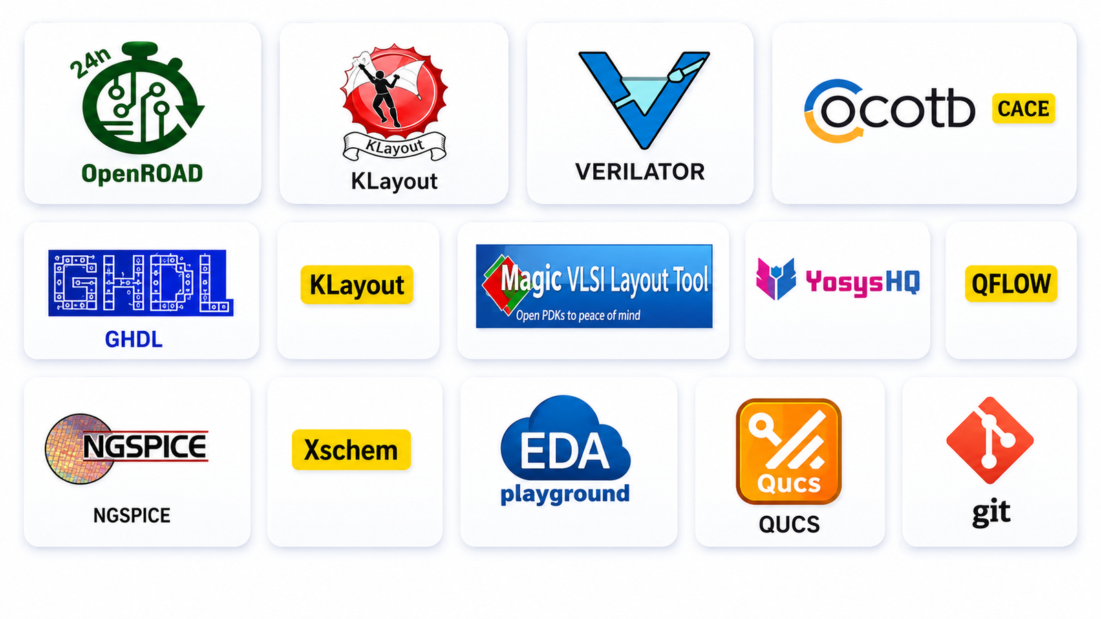
Open-Source Tools & Technologies Used
Top Job Roles
VLSI Design Engineer ASIC Design Engineer FPGA Design Engineer Physical Design Engineer RTL Design Engineer Verification Engineer Analog IC Design Engineer
Top Recruiting Companies in India
Intel AMD NVIDIA Qualcomm Texas Instruments Wipro HCL Technologies Tata Elxsi Sankalp Semiconductor Saankhya Labs Open-Silicon eInfochips
Career Prospects
📈 Rapid Semiconductor Market Growth
India’s semiconductor industry is projected to exceed $100 billion by 2030, creating significant demand for VLSI professionals across design, verification, and manufacturing.
India’s semiconductor industry is projected to exceed $100 billion by 2030, creating significant demand for VLSI professionals across design, verification, and manufacturing.
Source: Finance India News
🏭 Government Semiconductor Mission
Government initiatives and investments in semiconductor manufacturing are generating thousands of new opportunities in chip design and electronics engineering.
Government initiatives and investments in semiconductor manufacturing are generating thousands of new opportunities in chip design and electronics engineering.
Source: Reuters
💼 High-Demand Career Opportunities
Growing demand for ASIC, FPGA, Physical Design, AI Hardware, Automotive Electronics, and IoT Chip Design engineers ensures excellent salaries and long-term career growth.
Growing demand for ASIC, FPGA, Physical Design, AI Hardware, Automotive Electronics, and IoT Chip Design engineers ensures excellent salaries and long-term career growth.
Source: LinkedIn & Leap Robots
Module 1: VLSI Fundamentals & Industry Trends
Module 2: Digital VLSI Design & RTL Implementation
Module 3: Analog & Mixed-Signal VLSI Design
Module 4: FPGA & SoC-Based Design
Module 5: ASIC Physical Design (PD)
Module 6: Design Verification & UVM
Module 7: 3D ICs & Advanced SoC Architectures
Module 8: Industry-Specific VLSI Applications
Module 9: Industry Expert Sessions
Module 13: Certification Exam
Please, login to leave a review